

MATEL

Eurostarts

Biowings

DigitUS
PiLOC

Innosuisse
MATEL
Budget: 700’000 CHF
Program: HORIZON-CL4-2022-RESILIENCE-01
Status: Ongoing

innovations for advanced opto-Electric applications in AR and biosensing
MatEl builds upon advanced materials and beyond the state of the art digital processing technologies to enable new integration schemes fostering the wide adoption of hybrid OEICs to industrial and biomedical applications: Laser Digital Processing - Laser Transfer and Laser Soldering - will be employed as a key enabling technology for the accurate and fast alignment & bonding of any type of chip package (PIC and IC) on the innovative hybrid Si3N4 platform. The hybrid platform will be enhanced by the monolithic integration of advanced materials (e.g. graphene and high-quality PZT) which will enable multiple functionalities in miniaturized footprint, for the next generation of optoelectronic applications.
MatEl’s objective is to introduce novel integration schemes enabled by laser processing of advanced materials and enable the digital bonding of heterogeneous components for the next generation of OEICs.
Wafer – scale integration of high-quality and defect-free advanced materials
Hybrid Si3N4 wafer platform featuring etched pockets compatible with heterogeneous active components (III-V, II-V chips and electronic chips)
First fully digital, laser-based wafer processing and die-bonding
Generic housing for hybrid OEICs with diverse functionalities
Demonstration of two optoelectronic end-applications.

PiLOC
Budget.100’000 EUR
Program: Launchpad
Status: finished
Problem: the need for high speed, flexible, multiparametric systems are challenging the technological and cost constraints. Indeed, an increasing number of discrete components like actuators and valves can already be implemented on glass, but who is willing to spend up to 500€ for a disposable chip?
Proposed solution: novel technology for the seamless integration of valves, pumps, and injectors made with piezoelectric thin films onto polymer microfluidic chips, thus leading to the next generation of low cost and high performance LOC. This will allow monolithic fabrication of LOC using MEMS technology, benefiting from the advancements in MEMS manufacturing and the facilities available at EPFL.
Microfluidics technology has revolutionised key applications like drug development, stem cell research, microbiological analysis, medical diagnosis, personalised medicine and chemical biology, just to name but a few. Microfluidic systems are ever more present in chemistry and biochemistry labs, driving the development of new components and processes for the injection, mixing, pumping, and storing of fluids in microchannels.
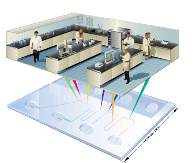
Lab-On-a-Chip for advanced Diagnostics

Successfully transferred AlScN film onto Su8 layer
DigitUS
Budget.100’000 EUR
Program: Launchpad
Status: finished
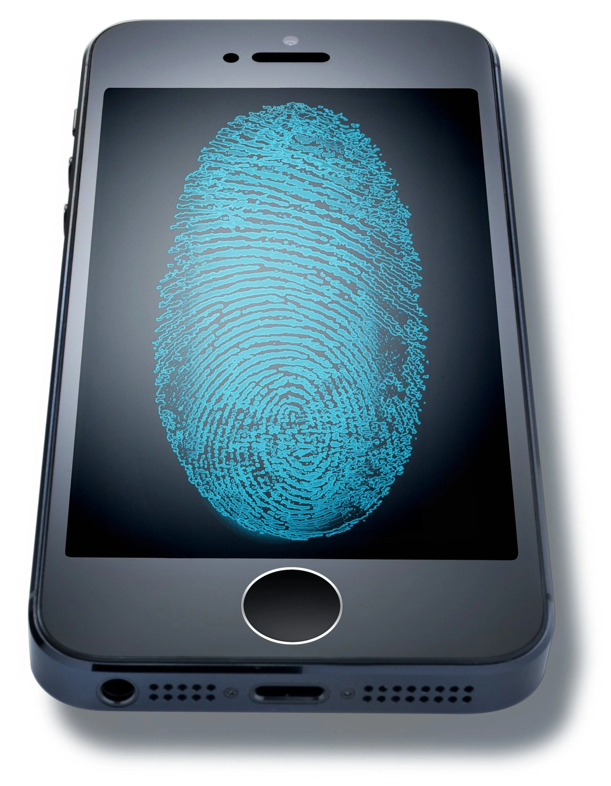
Problem: With the world progressively going digital, digital security is the main concern and our daily experience highlights two main issues with respect to fingerprint sensors: 1) Reliability of the fingerprint sensor is a major issue, as capacitive fingerprint sensors can be easily spoofed. Besides, failures in recognising the fingerprint undermines the user experience. 2) Form factor: fingerprint sensors take a vital space of the display, challenging the ongoing trend of borderless consumer electronics.
Proposed solution: we proposed a solution based on PZT (Lead Zirconate Titanate), that is at least 10 times stronger than the materials currently used for integrated ultrasound scanners. PZT can be readily integrated into micro-electromechanical systems (MEMS), which paves the way to the adoption of the solution into mainstream applications. Besides, the technology has the possibility to be integrated under many different materials such as glass, sapphire and even some metals, with the possibility to operate along the entire screen surface, thus not limiting fingerprint detection to a specific location.
The use of fingerprints for personal identification dates back to the ninetieth century, while its digital integration into every day devices is relatively new. Fingerprint authentication is more secure and convenient than passwords for modern electronics, making this technology an increasingly common feature in smartphones, tablets and in a host of other applications.
Under screen finger print scanner
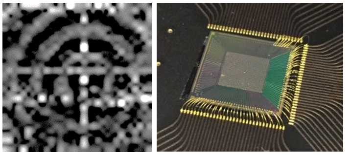
A close-up view of the chip (bottom-right) and an image of a circular pattern obtained with the prototype

Biowings
Budget.316’000 EUR
Program: FETOPEN
Status: finished
BioWings proposes to solve this deadlock through the implementation of a completely new class of smart actuating materials to be integrated in biocompatible MEMS. This family of materials is based on highly defective cerium oxides, which recently displayed radically different properties compared to existing ones:
They are non-toxic and environmentally friendly, unlike the current lead-based actuators;
They show exceptionally high and still uncapped electrostrictive response under moderate electric fields, enabling low power consumption devices;
They are fully compatible with silicon-based technologies and many other substrates, including metals and polymers.
Demographic trends, such as the rapid growth and ageing of the world population, are putting pressure on global healthcare systems, increasing the demand for smart, effective and affordable biomedical systems. Micro Electro-Mechanical Systems (MEMS) are key components of such biomedical systems, enabling miniaturised devices with diagnostic, prognostic and therapeutic functionalities. Although these systems are poised to revolutionize medical diagnostics and treatment approaches, the slow progress in the development of biocompatible actuator materials is still hindering this industry, preventing a host of new biomedical devices to enter the mainstream market.
Biocompatible electrostrictive smart materials for future generation of medical micro electro-mechanical systems
Piezoelectric stack, on Si/glass chips. developed and fabricated by Piemacs
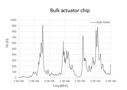
Resonance peaks in bulk transducer (old solution)
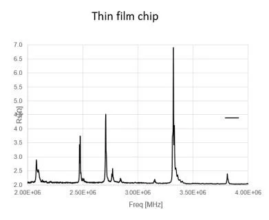
Resonance peaks in bulk transducer (Piemacs’s solution)
CBVD-4-MEMS
Budget: 300’000 CHF
Program: Eurostars 3 - Call 2
Status: Ongoing
PZT shows the highest piezoelectric coefficients among thin-film materials. Their use in piezo-MEMS is fast increasing for commercial applications in high-volume health, consumer, and IoT markets. Wafer-scale PZT films are deposited by three main techniques: chemical solution (SolGel), magnetron sputtering, and pulsed laser deposition (PLD). All three techniques have serious drawbacks.
The goal: grow PZT and Pt thin films through laser-assisted CBVD (Chemical Beam Vapour Deposition) to simultaneously improve overall material quality, uniformity, and performance in a mass-production approach.
The agile additive growth technique enables new thin-film architectures such as complex layer stacks with variable composition or alternating Platinum electrodes.
CBVD deposition and optimization of perovskite based piezoelectric thin films for IoT

48336.1 IP-ENG
Innosuisse contribution: 197’820 CHF
Program: MEMS & MOEMS & BIOMEMS
Status: finished
PZT thin films show the highest piezoelectric coefficients among thin film materials. Their use in MEMS sensors and actuators (called piezo-MEMS) is seeing an increasing number of applications reaching commercial maturity in high-volume consumer and IOT markets. PZT thin-films are deposited by three main techniques: Chemical Solution Deposition (CSD), sputter deposition and Pulsed Laser Deposition (PLD). The industry has a strong request for industry-level PLD processes, promising a number of advantages over CSD: higher throughput, lower materials costs, lower deposition temperature and self-poling options. Self-poling does not only reduce the complexity of device fabrication, it also means a more stable polarisation, and thus a higher performance at low electric fields. This is important for all sensors and low-voltage applications, such as hearing aids.
New solutions for fast growing piezoelectric thin film demand for internet of things (IOT)
This project aims to establish Piemacs as supplier of PZT thin films deposited by PLD by solving the current limitations:
(1) Growth of PLD-PZT on patterned platinum electrodes. Such capability is a must for high-performance piezoelectric structures.
(2) Processes and layer designs leading to self-poling.
48336.1 IP-ENG
Innosuisse contribution: 197’820 CHF
Program: MEMS & MOEMS & BIOMEMS
Status: finished
High performance piezoelectric Micromachined Ultrasonic Transducer for finger print detection
Piezoelectric MEMS components are essential ingredients for new sensors and transducers for the industry 4.0 and the Internet of Things (IoT) and connected consumer electronics. The project idea is to develop a novel Piezoelectric Micro-Machined Ultrasound Transducer (pMUT), for finger print detection that has unbeatable advantages over capacitive recognition, which is currently dominating the market. This will be achieved by using a strong piezoelectric thin film, PZT (lead zirconate titanate), along with a new combination of electrode and innovative driving circuit design. The project will be benefiting from all the recent advancements in piezoelectric thin film synthesis, microfabrication, and finite element modeling. This project will help PIEMACS to evolve into a MEMS component supplier, and will generate more know-how in the biometric and medical imaging markets. The electrode design and the novel circuit to drive the pMUT, proposed together in this project, will also have further impacts for PZT-based piezoMEMS devices. This project extends the activity of PIEMACS, and will help it to grow and hire more personnel. It is expected to bring in more customers, and also from other applications fields. PIEMACS is in contact with many big and small players in the market of piezoelectric MEMS. Based on our know-how, we helped customers from different markets to develop or improve their products for various applications. PIEMACS has discussed the proposed project with several partners. All of them, and also a private investor, confirmed their interest in the proposed project. All of them have interest to integrate the novel pMUT in their applications.