

Piezoelectric thin film analysis
-
4 point bending technique
Full test structure fabrication
Mapping over the wafer
-
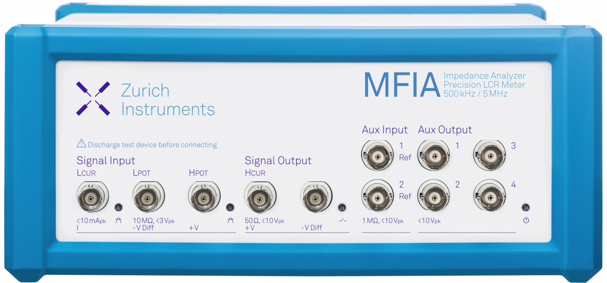
Large and small signal
Full test structure fabrication
Mapping over the wafer
-
From mHz to GHz
Full test structure fabrication if needed
C-V and P-V loops
Large and small signal measurement
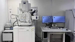
Microstructural thin film analysis
-
EDAX
-
XRD
SEM
TEM
FIB
Ceramic pallet analysis